The M17 Nokia 3310 (Part 1)
Posted on 2025-06-22After Wojciech SP5WWP posted on LinkedIn that you can now order pre-assembled PCBs for the M17-3310 project on PCBWay, I took a closer look at the project. This is a circuit board that can be installed in an old Nokia 3310 instead of the original mainboard. This board enables FM/FSK/M17 communication on the 70cm band and turns the good old 3310 into an interesting toy in conjunction with the M17 project. Currently there is a simple firmware that provides M17 messaging support with T9 text entry method. “The device can be powered with original Nokia lithium-ion batteries or their replacements and is able to charge them through the USB-C port. A UART USB interface is available, allowing the device to work as an RF modem.”
Sourcing
I have to admit that I didn’t understand PCBWay’s ordering process, so I decided to just order the bare PCB from JLCPCB, who I’ve had good experiences with so far. To do this, I downloaded the Gerber files here and used them to have 5 PCBs manufactured by JLCPCB.
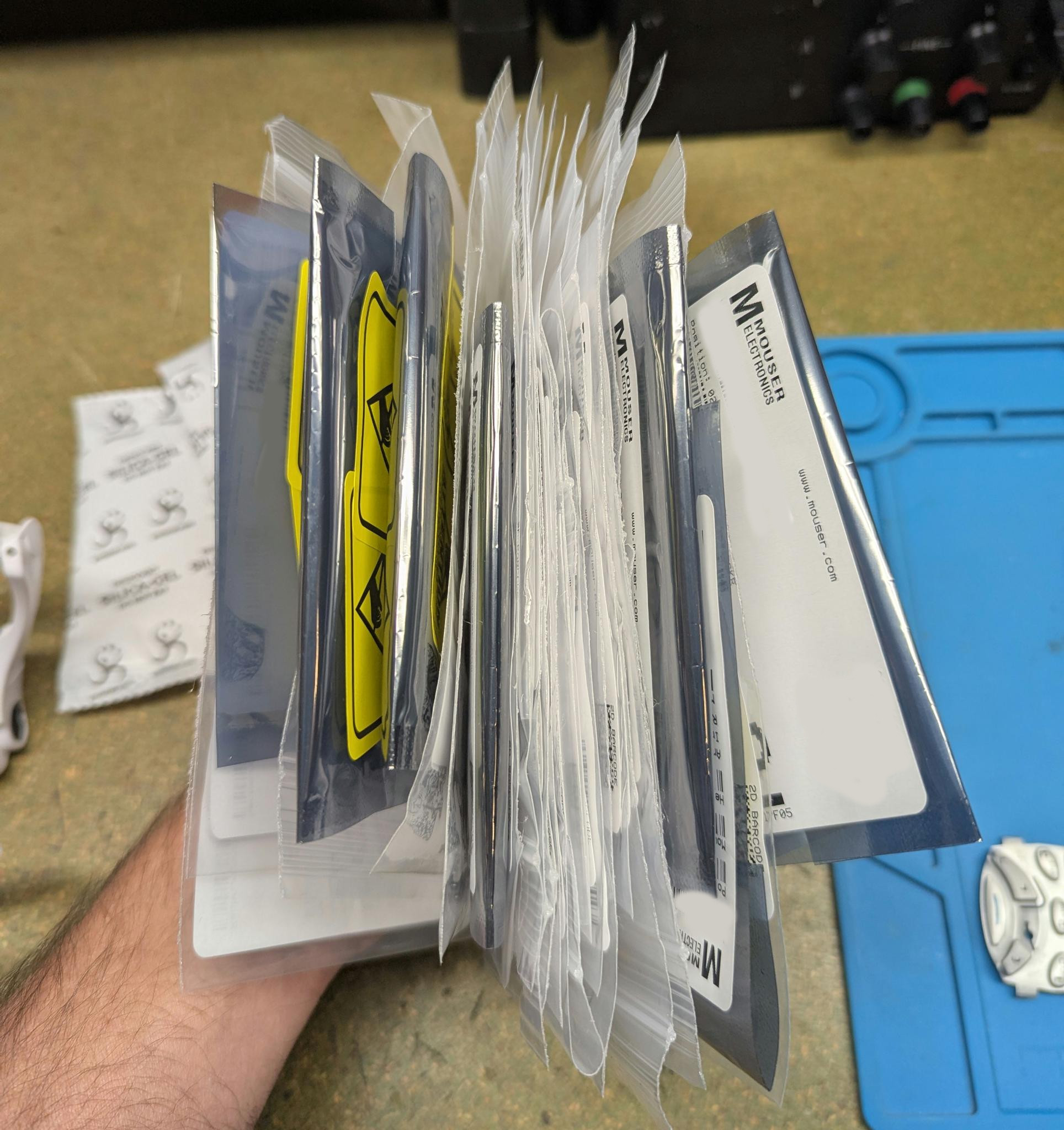
I then downloaded the BOM from the same site and ordered almost all the necessary components from Mouser. The only component not available there is the G-NiceRF SA868S UHF RF module to which the OpenRTX firmware will be flashed later. I was able to order this from AliExpress.
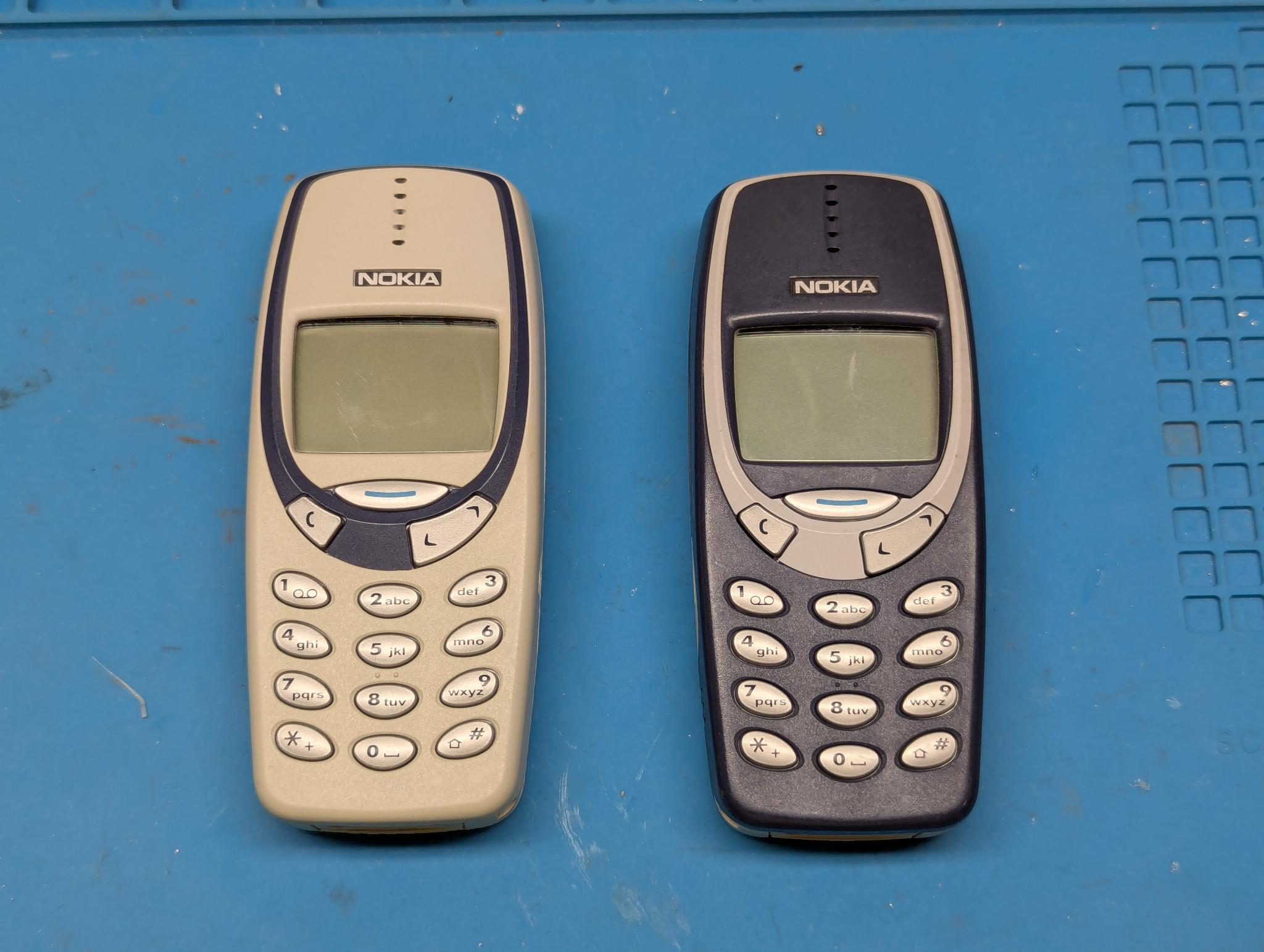
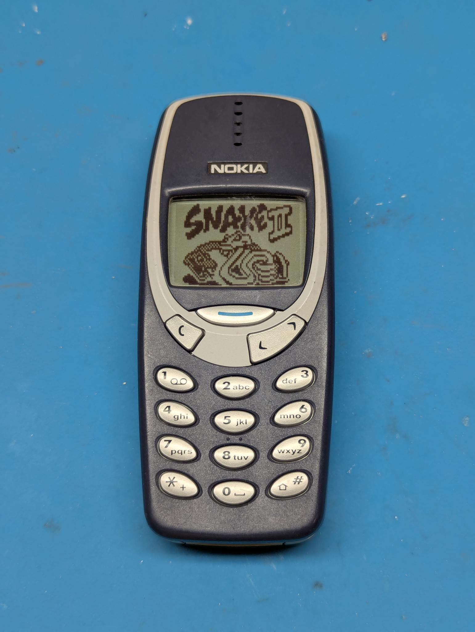
Last thing missing is of course a Nokia 3310 or 3330. As i didn’t own either model, i bought both a 3310 and a 3330 second-hand. Of course, one phone is enough, but one of the two was so cheap that I had to go for it.
Nokia Disassembly
When I dismantled the Nokia, I realized how ingenious the basic idea of the project is and how great the phones of the 2000s were built.
Here is a picture of both devices unopened:
First remove the rear cover by pressing the lower button on the back and pushing up the cover:
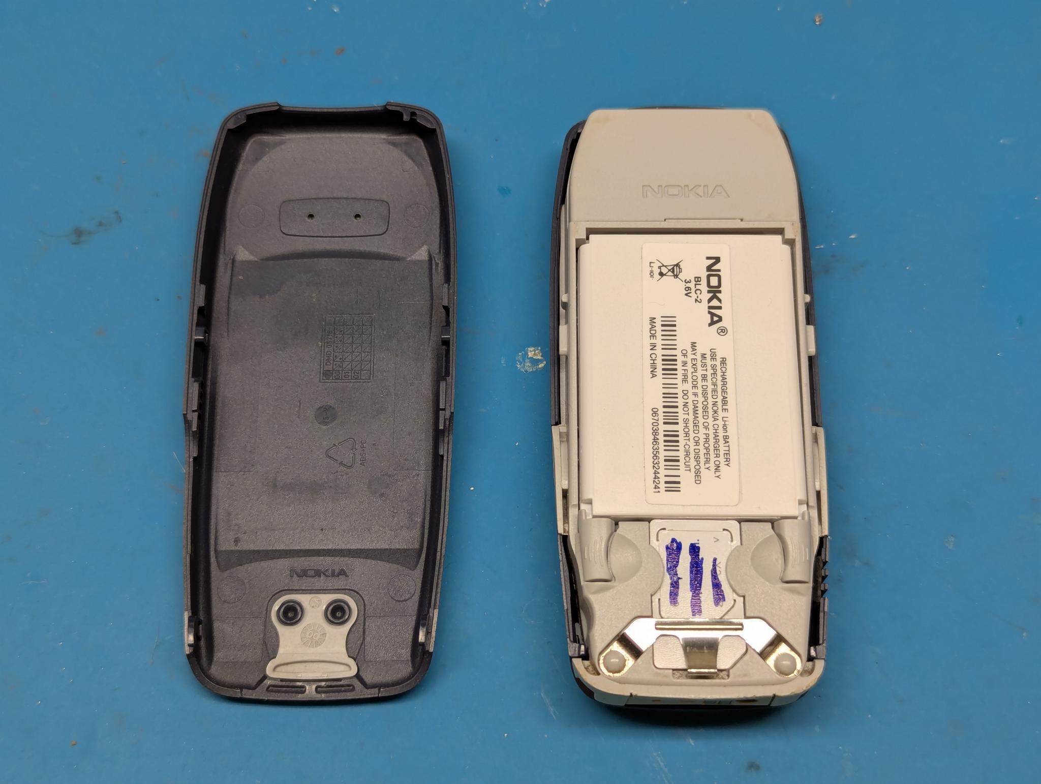
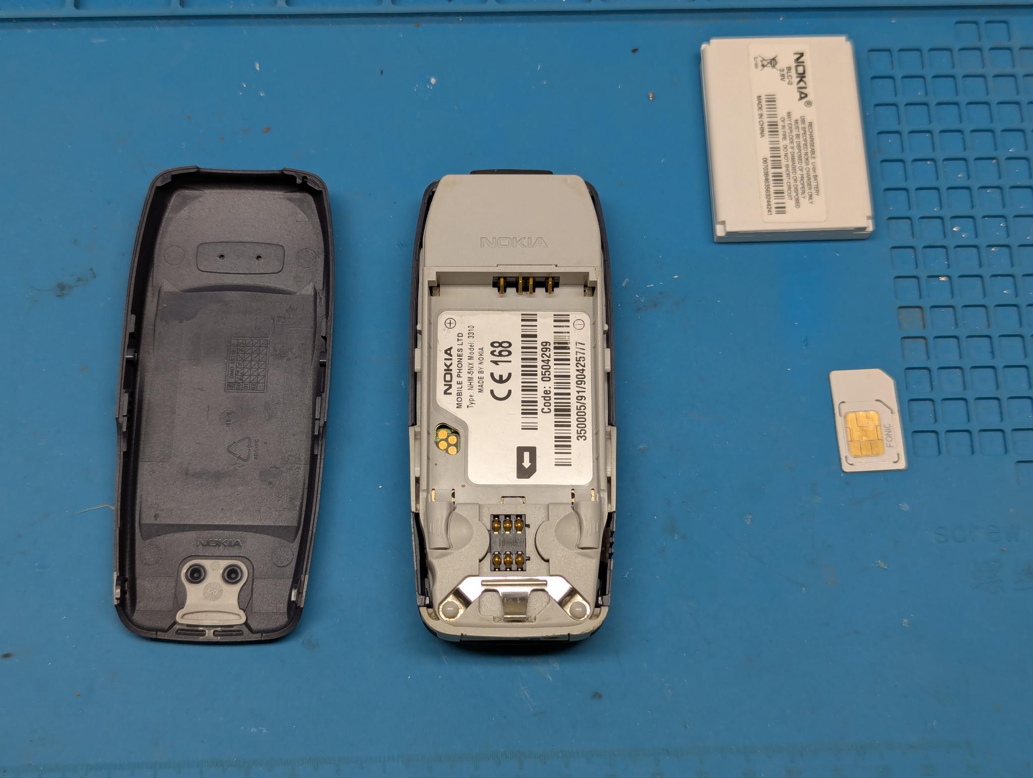
Then the battery and SIM card can be removed:
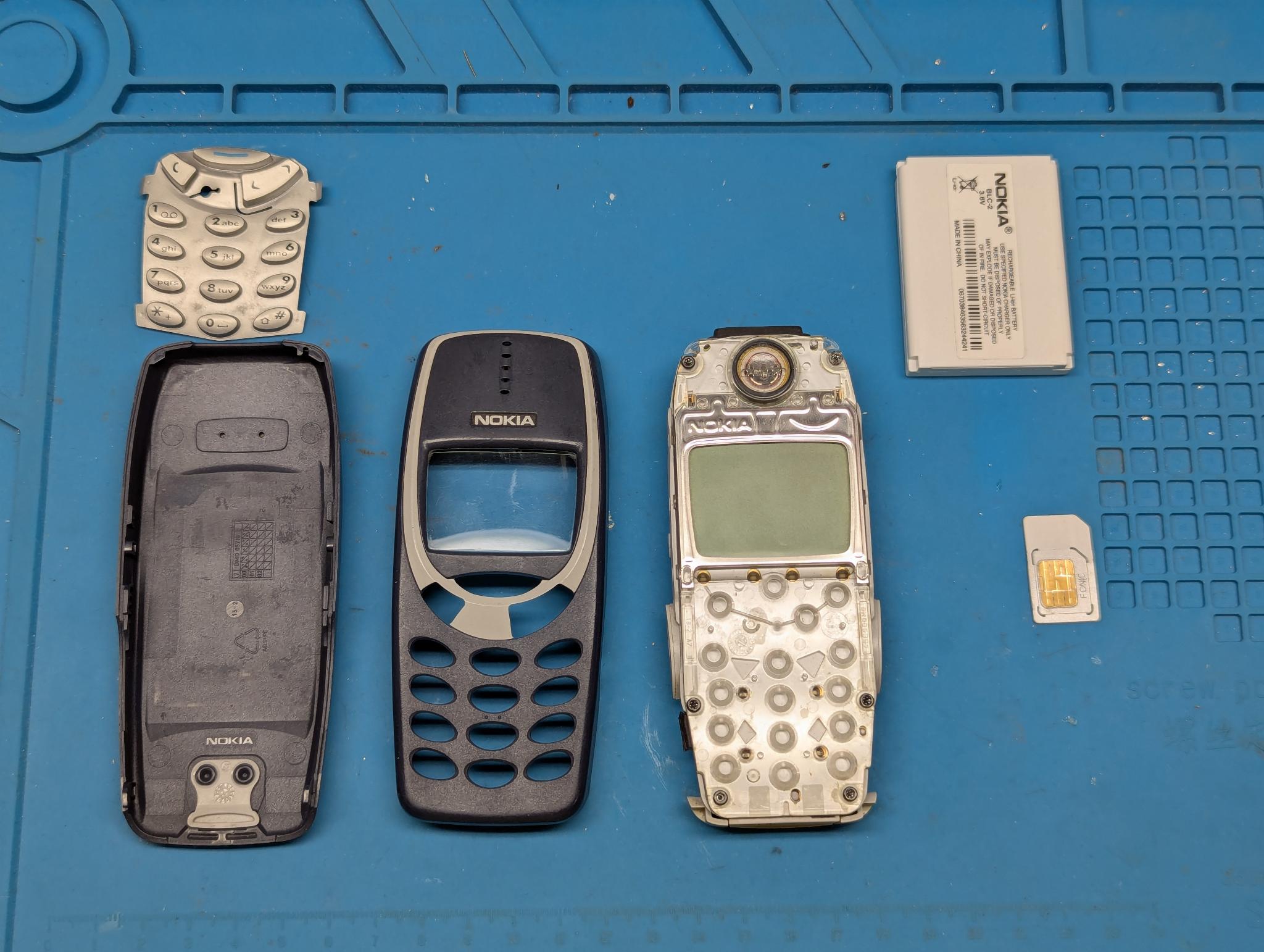
The front cover can then be removed by simply levering it off to the side. The keyboard foil will fall out:
Now the PCB can be removed from the module above by loosening the 6 Torx T6 screws:
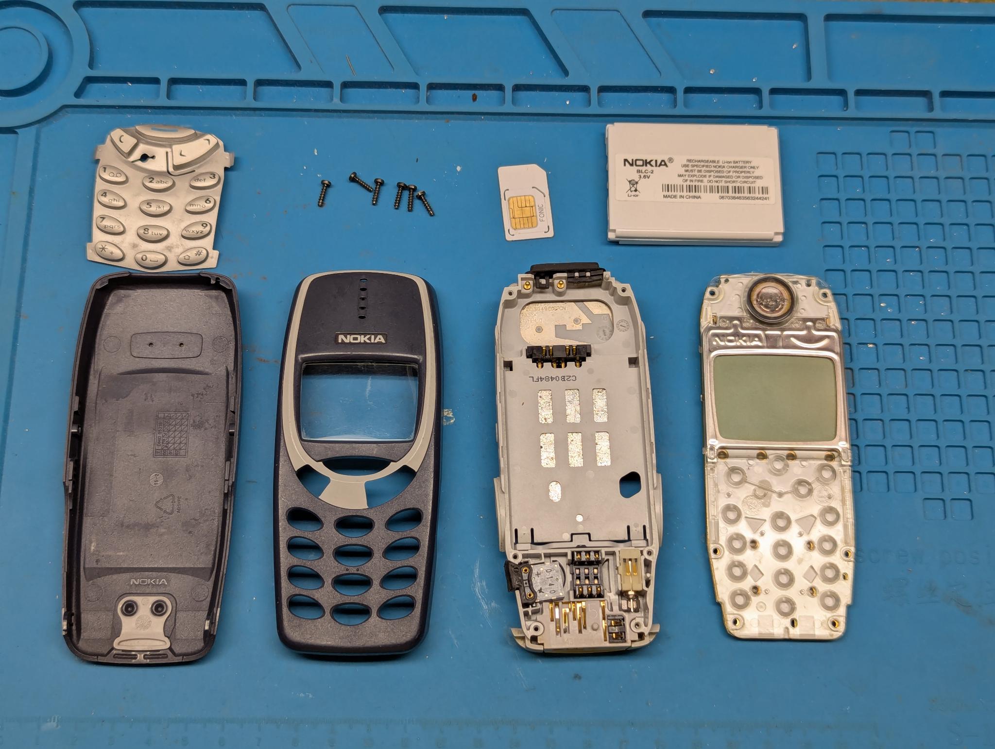
Here is a final picture of all the components in the order in which they are assembled:
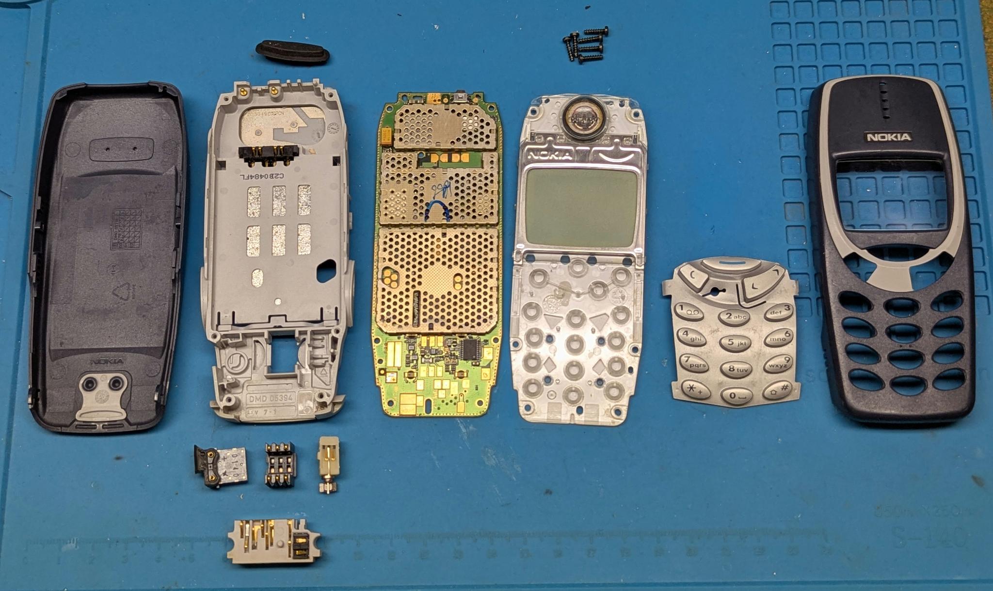
It is easy to see that apart from the 6 Torx screws, everything is not only modular but also connected to each other without screws and cables by spring contacts. In the past, if only the vibrator broke, for example, it was very easy to replace it. Unfortunately, those days are over.
Preparations
Before I would be able to solder, I first had to find out which components go where. First of all, I created a list of all the components based on the downloaded BOM:
| Designator | Value | Description |
|---|---|---|
| C1, C2 | 6p8 | Unpolarized capacitor |
| C10, C12, C13, C19, C5, C6, C7, C8, C9 | 100n | Unpolarized capacitor |
| C11, C17, C18 | 47uF/10V | Polarized capacitor |
| C14, C15, C16 | 10uF/10V | Polarized capacitor |
| C20 | 10n | Unpolarized capacitor |
| C21, C22 | 20p | Unpolarized capacitor |
| C3, C4 | 2u2 | Unpolarized capacitor |
| D1, D2, D3, D4, D8 | BAT60A | 10V 3A High Current Recitifier Schottky Diode, SOD-323 |
| D10, D11, D12, D13, D5, D6, D7, D9 | RED | Light emitting diode |
| FB1, FB2, FB3 | Bead | Ferrite bead |
| FL1 | LFCN-490+ | 490MHz 50 Ohm Passive Low Pass Filter, FV1206 |
| J8 | USB C | USB 2.0-only 16P Type-C Receptacle connector |
| L1 | 1u5 | Inductor |
| Q1, Q3, Q4, Q5, Q7 | BSS138 | 50V Vds, 0.22A Id, N-Channel MOSFET, SOT-23 |
| Q2, Q6 | IRLML6401 | -4.3A Id, -12V Vds, 50mOhm Rds, P-Channel HEXFET Power MOSFET, SOT-23 |
| R1, R6 | 22k | Resistor |
| R10, R13, R15, R17, R20, R7, R8 | 100k | Resistor |
| R11, R12, R18, R3, R31, R32, R33, R34, R35, R4, R9 | 47k | Resistor |
| R14, R28 | 1k | Resistor |
| R16, R19, R21, R22, R23, R24, R25, R26, R27 | 56R | Resistor |
| R2 | 2k2 | Resistor |
| R29, R30 | 5k1 | Resistor |
| R5 | 10k | Resistor |
| SW1 | POWER ON/OFF | |
| U1 | STM32F405RGTx | STMicroelectronics Arm Cortex-M4 MCU, 1024KB flash, 192KB RAM, 168 MHz, 1.8-3.6V, 51 GPIO, LQFP64 |
| U3 | MAX1555 | |
| U4 | MAX16054 | |
| U5 | TPS63031DSK | Buck-Boost Converter, 1.8-5.5V Input Voltage, 1A Switch Current, Adjustable Output Voltage, VSON-10 (DSK0010A) |
| U6 | USBLC6-2SC6 | Very low capacitance ESD protection diode, 2 data-line, SOT-23-6 |
| Y1 | 8MHz | Four pin crystal, GND on pins 2 and 4 |
The first hurdle I encountered was that I couldn’t find any documentation on where to place which components on the PCB. Wojciech then pointed out to me that this information can be found in the KiCad project files, which are part of the project on GitHub. I generated the following simplified image with the respective locations of the components:
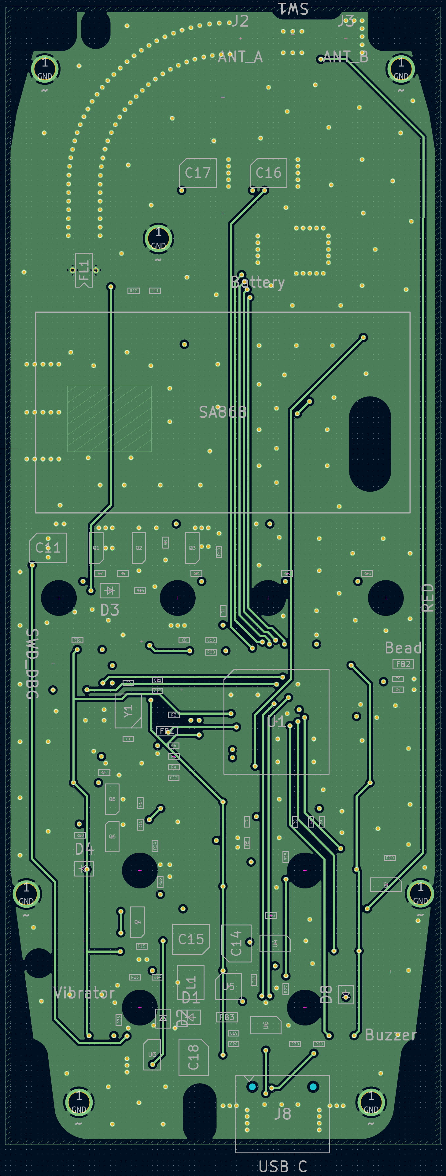
You might want to right-click on the above image to open it in a separate tab since some texts might be otherwise hard to read.
Update:
One big advantage of doing this project is that I learned some new things about KiCad. In this case I’ve learned that there is a plugin available, that creates an interactive HTML BOM viewer. The version I’ve created can be found here on my server. You might want to click on “F” on the top right as there will be no components placed on the back of the PCB.
More Purchases
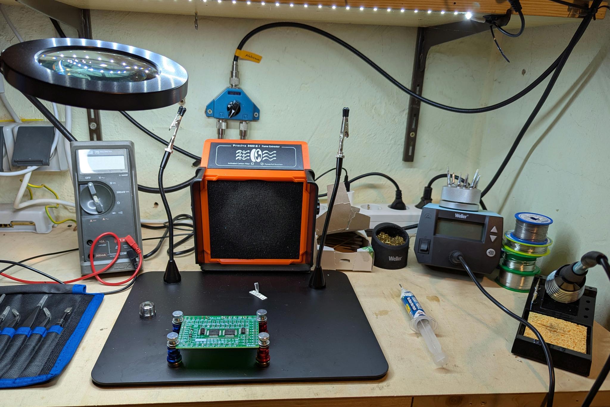
These types of projects can be very expensive. For example, if you are afraid of soldering the smallest SMD components, you might consider buying a good magnifying glass with light or even a new soldering station. No matter how the project turns out, my electrical tinkering corner in the workshop has been significantly improved.
Conclusion of Part 1
In the meantime, I have received all the components I ordered, prepared everything for the assembly of the circuit board and have two Nokias on hand:
All that’s missing now to actually get started is the PCB, which has already been manufactured but is still in transit. Until then, the only thing left to do is to find a meaningful occupation:
Part 2 of this project will be the biggest challenge for me: soldering many small and sometimes multi-legged SMD components…